+965 51122049

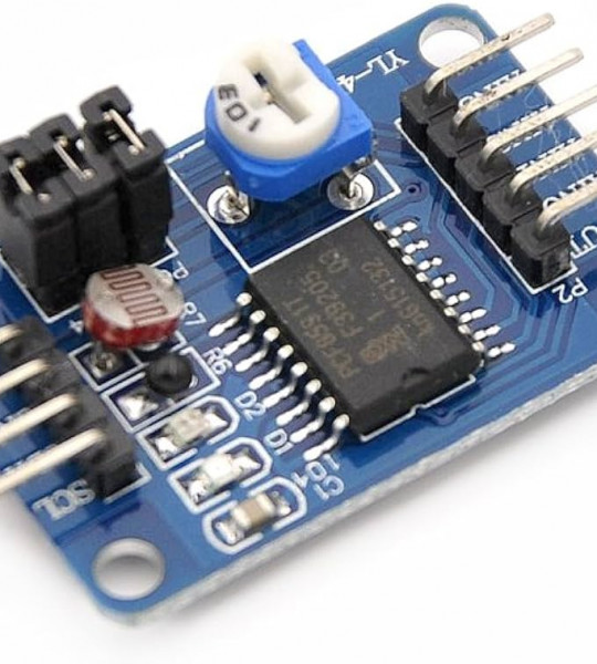
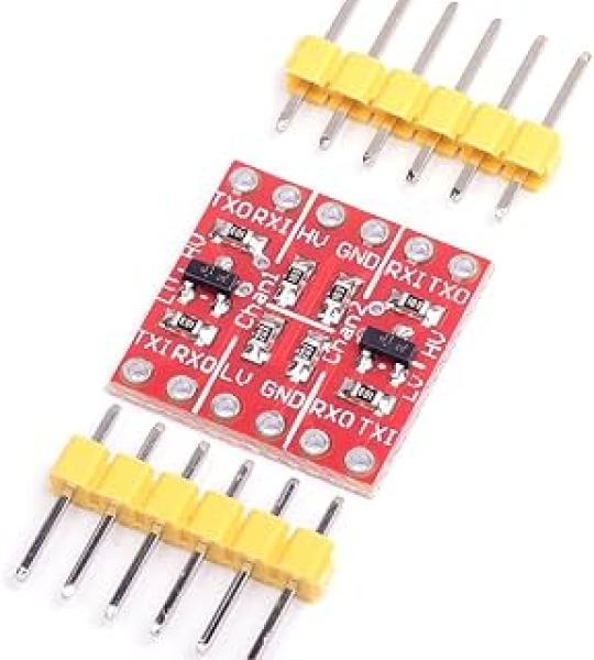
Module Description:
Wiring instructions:
Left 4 pin:
Right 8 pin :
Your email address will not be published. Required fields are marked *
Please login to write review!
Looks like there are no reviews yet.
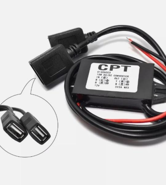
DC-DC step-down 12V to 5V dual USB car power converter 3A 15W
Logic Level Converter 3.3V 5V TTL for Arduino
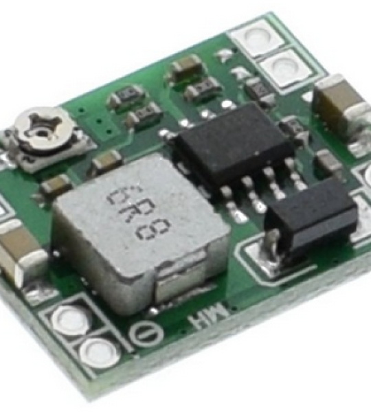
MP1584EN DC-DC Buck Power Module 3A Adjustable buck module
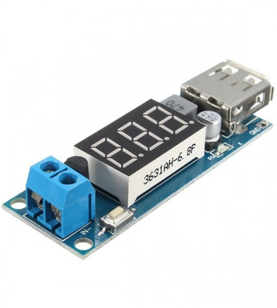
DC 4.5- 40V to 5V 2A USB Charger dc-dc step down Buck converter voltmeter module