+965 51122049

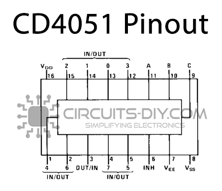
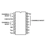
| Pin No | Pin Name | Description |
|---|---|---|
| 1 | I/O 4 | channel 4 i/o |
| 2 | I/O 6 | channel 6 i/o |
| 3 | O/I | common i/o |
| 4 | I/O 7 | channel 7 i/o |
| 5 | I/O 5 | channel 5 i/o |
| 6 | INHIBIT | disable all channel |
| 7 | VEE | Emitter supply |
| 8 | VSS | source supply |
| 9 | C | input c |
| 10 | B | input b |
| 11 | A | input a |
| 12 | I/O 3 | channel 3 i/o |
| 13 | I/O 0 | channel 0 i/o |
| 14 | I/O 1 | channel 1 i/o |
| 15 | I/O 2 | channel 2 i/o |
| 16 | VDD | Drain supply |
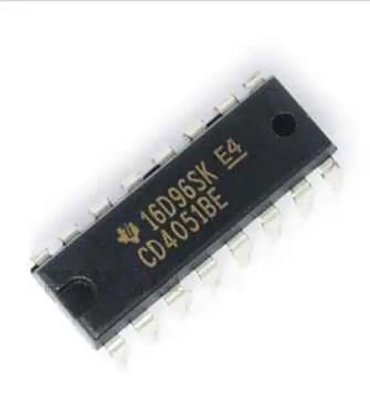
You can download the datasheet for CD4051 Single 8-channel Multiplexer/Demultiplexer from the link given below:
Your email address will not be published. Required fields are marked *
Please login to write review!
Looks like there are no reviews yet.
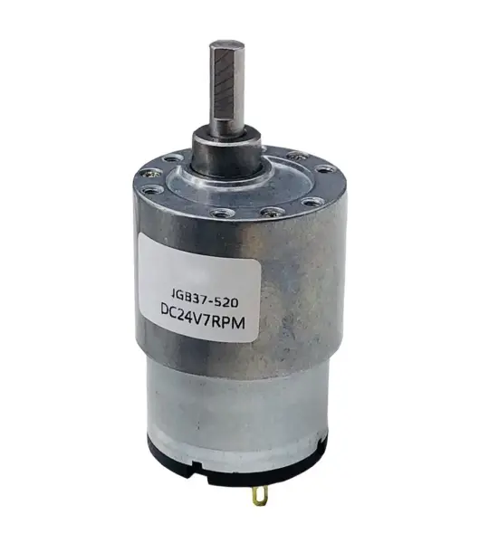
DC 24V 7RPM 37mm Diameter JGB37 520 eccentric Shaft Geared Industrial Grade Highly Reliable and Full Copper Motor
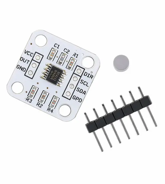
as5600 magnetic encoder magnetic induction angle measurement sensor module
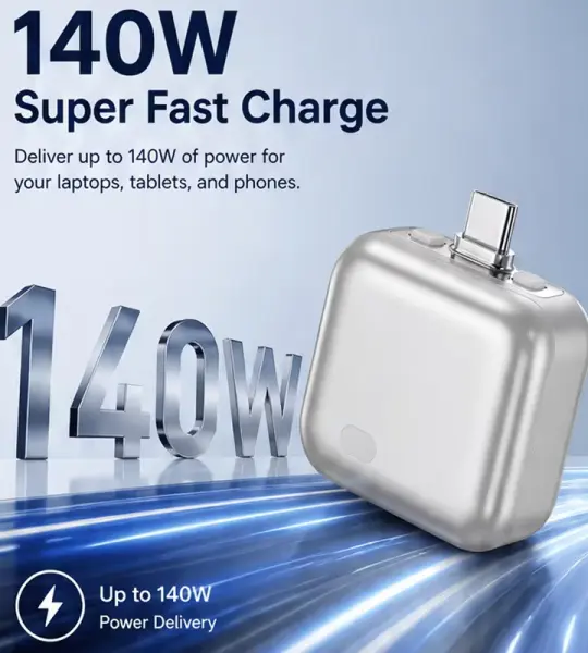
Type-C Smart Auto-Power-Off Charger Adapter, Full-Charge Auto Cutoff Intelligent Power Protector
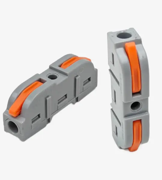
Single Pole Wire Connector 0.08 to 2.5mm Terminal Block with Spring Lock Lever for Cable Connection