+965 51122049

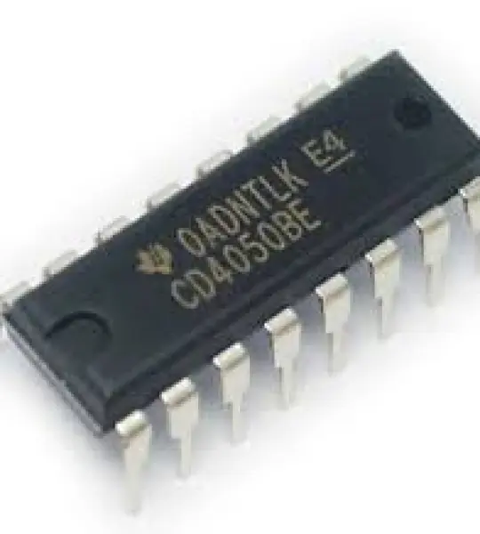
The CD4050 IC is a hex buffer chip with six non-inverting buffers that pass signals unchanged, ideal for voltage level conversion and signal regeneration. It can drive up to two TTL or DTL devices at once, offering reliable performance with low power consumption. Its high sink current capability ensures it handles multiple loads efficiently, making it a versatile choice for digital circuits.
This section provides the key highlights and specifications of the CD4050 IC, including its operating voltage, current consumption, and performance metrics.
| Parameter | Specification |
| Operating Voltage | 3V - 15V DC |
| Current Consumption (Max) | 50mA |
| Sink Current Capability | High Sink Current for Driving 2 TTL Loads |
| Maximum Low-Level Output Voltage | 0.5V at 5V Vcc |
| Minimum High-Level Output Voltage | 4.95V at 5V Vcc |

| Pin Number | Pin Type | Description/Direction |
| 1 | VCC | Positive input supply |
| 2 | G | Non-Inverted output 1 |
| 3 | A | Input 1 |
| 4 | H | Non-Inverted output 2 |
| 5 | B | Input 2 |
| 6 | I | Non-Inverted output 3 |
| 7 | C | Input 3 |
| 8 | VSS | Negative Supply |
| 9 | D | Input 4 |
| 10 | J | Non-Inverted output 4 |
| 11 | E | Input 5 |
| 12 | K | Non-Inverted output 5 |
| 13 | NC | No connection |
| 14 | F | Input 6 |
| 15 | L | Non-Inverted output 6 |
| 16 | NC | No connection |
The CD4050 IC is designed with non-inverting buffers that maintain the input signal as it is, without changing its logic state. Unlike an inverter, which flips the signal, a non-inverting buffer ensures the output matches the input. Its primary purpose is to strengthen the signal, delivering a clear HIGH or LOW at the output.

Each buffer within the IC has a single input and a single output. The output is always equal to the input, making it suitable for applications where signal integrity needs to be preserved. These buffers can also introduce a slight propagation delay, which can be useful in specific circuit designs.
Your email address will not be published. Required fields are marked *
Please login to write review!
Looks like there are no reviews yet.
LM833N DIP-8 Amplifier Audio Integration Dual Operational Amplifiers