+965 51122049

ESD Control Selection Guide V1
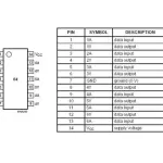
Schematic Symbol & PCB Footprint
| Attribute | Value |
|---|---|
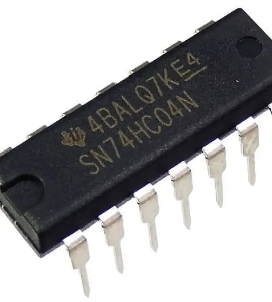
| Logic Function | Inverter |
| Number of Elements per Chip | 6 |
| Schmitt Trigger Input | No |
| Maximum Propagation Delay Time @ Maximum CL | 16 ns @ 6 V, 19 ns @ 4.5 V, 95 ns @ 2 V |
| Maximum High Level Output Current | -5.2mA |
| Maximum Low Level Output Current | 5.2mA |
| Mounting Type | Through Hole |
| Package Type | PDIP |
| Pin Count | 14 |
| Logic Family | HC |
| Dimensions | 19.3 x 6.35 x 4.57mm |
| Maximum Operating Supply Voltage | 6 V |
| Height | 4.57mm |
| Minimum Operating Temperature | -40 °C |
| Minimum Operating Supply Voltage | 2 V |
| Width | 6.35mm |
| Length | 19.3mm |
| Maximum Operating Temperature | +85 °C |
| Propagation Delay Test Condition | 50pF |
Your email address will not be published. Required fields are marked *
Please login to write review!
Looks like there are no reviews yet.